Description
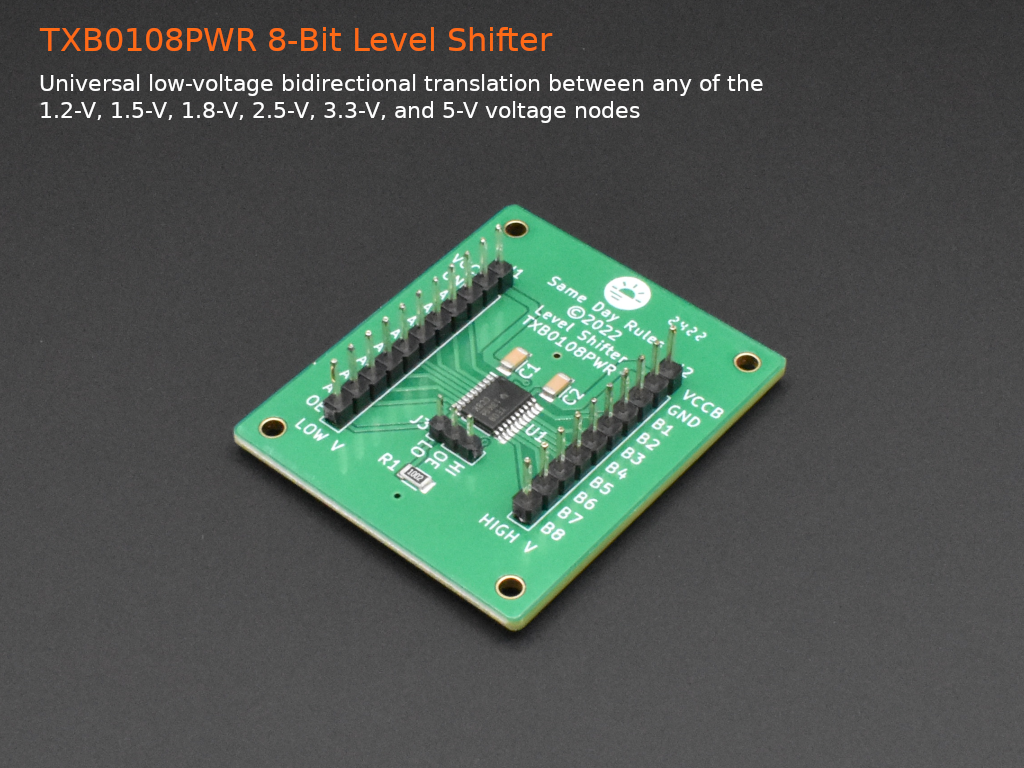
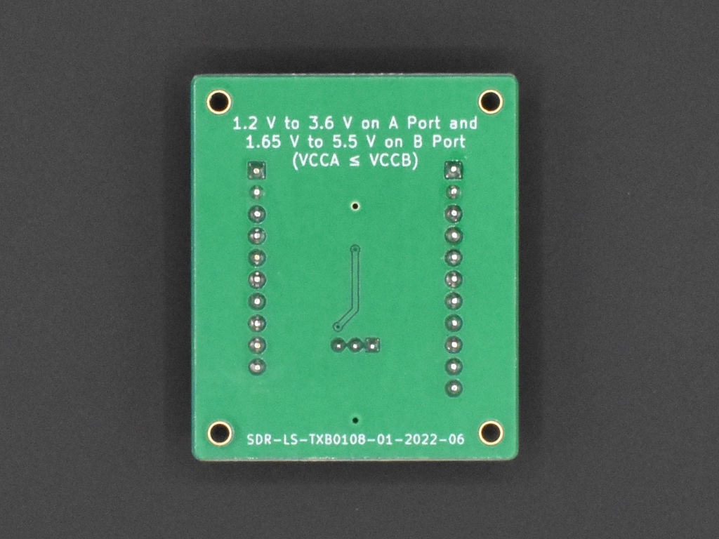
Eight-bit bidirectional voltage-level shifter with auto-direction sensing and ±15-kV ESD protection using the Texas Instruments TXB0108PWR. Provides an output enable (OE) line that controls the active state of the shifter. This eight-bit non-inverting translator uses two separate configurable power supply rails. The A port is designed to track VCCA. VCCA accepts any supply voltage from 1.2 V to 3.6 V. The B port is designed to track VCCB. VCCB accepts any supply voltage from 1.65 V to 5.5 V. This allows for universal low-voltage bidirectional translation between any of the 1.2-V, 1.5-V, 1.8-V, 2.5-V, 3.3-V, and 5-V voltage nodes. VCCA should not exceed VCCB. Maximum data rate between port A and B ranges from 20 Mbps (VCCA=1.2V) to 100 Mbps (VCCA=3.3V).
Note that the TXB0108PWR is a voltage-level shifter (i.e., not a logic-level shifter), mapping voltages received on one side of the device to voltages on the other side of the device. For example, if VCCA is provided 3.3V and VCCB is provided 5.0V, then a voltage of 3.3V applied to one of the VCCA signal pins (of J1) will be mapped to 5.0V on the corresponding signal pin on VCCB (of J2). Since logic levels on microprocessors vary in terms of actual voltage levels, it is not always the case that a logic-level signal applied to one side of the device will necessarily map to the same logic-level signal on the other side of the device.
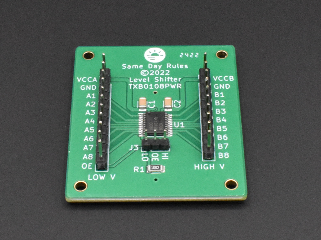
J1 connector is the low-voltage side with VCCA and GND signals at pins 1-2. Pins 3-10 are data bits 1-8 that are mapped to J2 pins 3-10 data bits 1-8. The voltages on J1 must be lower than the voltages on J2.
J2 connector is the high-voltage side with VCCB and GND signals at pins 1-2. Pins 3-10 are data bits 1-8 that are mapped to J1 pins 3-10 data bits 1-8.
J3 jumper block provides control over operation of the OE line. The OE input circuit is supplied by VCCA. Placing a jumper on J3 pins 1-2 pulls the OE line low to GND through a resistor so that the level shifter is disabled on power-up. This prevents spurious output on J2. The OE line can then be driven high by a logic high signal on J2 pin 11, which enables the device. Placing a jumper on J3 pins 2-3 pulls the OE line high to VCCA so that the level shifter is enabled on power-up. This is intended for use cases where an additional I/O bit is not available to control the OE line. Do not connect J3 pin 1 to J3 pin 3.
3D Model
Warning
This product involves the use of electrical power. Care must be taken to safeguard against personal injury (shock or electrocution) and the risk of fire. Make sure you are experienced with handling electrical power and know how to properly connect power cables, connectors, supplies, and interconnected equipment. Double-check the polarity of all power-related connectors before applying power.
Resources

Reviews
There are no reviews yet.